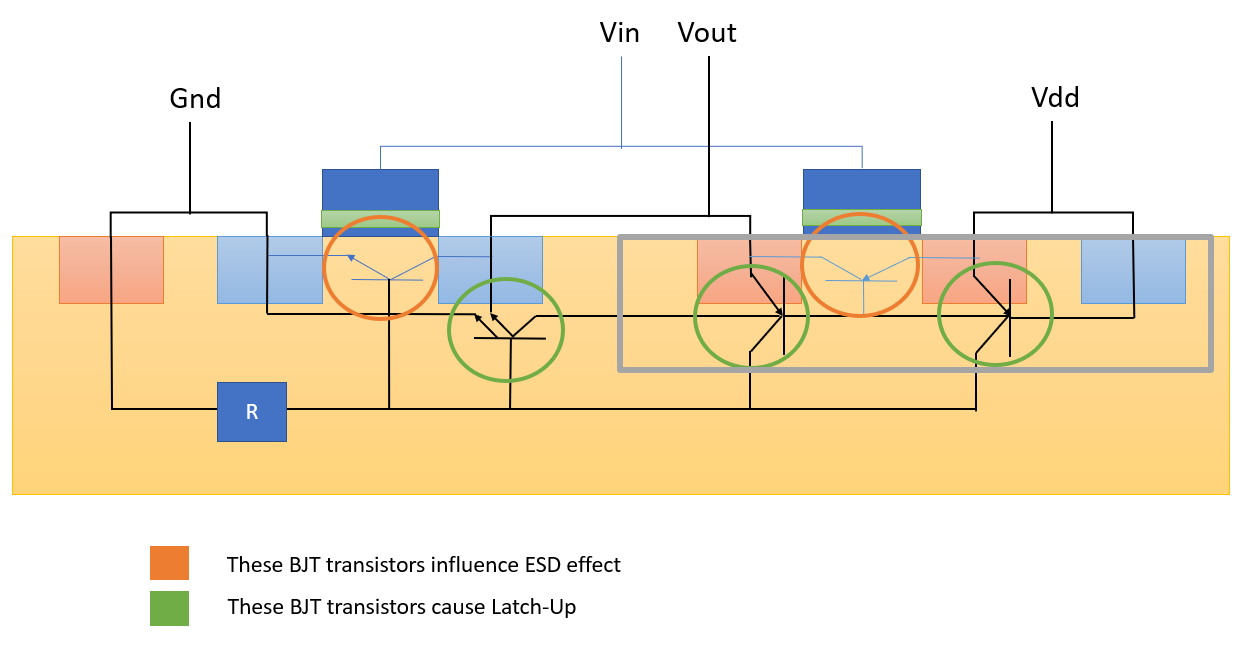
As can be seen in the above snapshot, resistance connected to the bases of NPN transistors and collectors of the PNP transistors greatly influences both ESD and Latch-Up effect in the layout. Furthermore, latch-up is sensitive to layout and hence most often solved at the layout level when doing the physical implementation of the design.
What is latch-up?
Latch-up is the creation of low impedance path between the power supply rails (e.g. vdd to gnd in the above case). It is caused when the parasitic BJT structures within an IC are triggered when a current/voltage is applied as stimulus in the input, output or I/O pin.
Sometime it also happen that the latch-up occur only while the pulse stimulus is connected to the IC and returns back to normal level once the stimulus is removed. Such an effect is called temporary (or) transient latch-up.
While a true latch-up is a one which remains even after the stimulus is removed. In such scenarios to remove the low impedance path between the power rails, a power supply shutdown is required.
How does it occur?
Latch-up is a regenerative process that occur when a pnpn structure (aka silicon controlled rectifier (SCR)) is formed. It is composed of parasitic npn and pnp transistor.

To avoid latch-up:
- Vpnpn <= Vs (Sustaining Voltage)
- Injecting current < Holding current (IH)
- Surround the transistor with guard rings.
- Reduce Rn and Rp. This will cause more current requirement for latch-up to occur.
Guard rings are used to collect majority (or) minority carriers flowing in the silicon. Tuning the doping level of the guard ring material helps in increasing or decreasing the resistance in the area of guard ring.
No comments:
Post a Comment